After sharing my last post on Reddit and Hackaday, I’ve gotten lots of kind feedback — and I deeply, deeply appreciate it all. More than anything else, it makes me regret not sharing this project with you sooner.
That said, the biggest ask has been for a detailed build guide. Unfortuantely, I didn’t document the build process in enough detail to write up a step by step guide, and I just don’t have the energy to build an entire new copy right now.
What I can do, however, is share discuss the design choices I made and share the build files. This post will focus on the hardware design of UNIAC, and I will follow it with a post detailing the software in greater detail.
Schematics
The schematic capture and layout was done in Eagle, and broken out into pages. It’s not perfect, by any means, but it’s clean enough.
Anyway, let’s go through the sections.
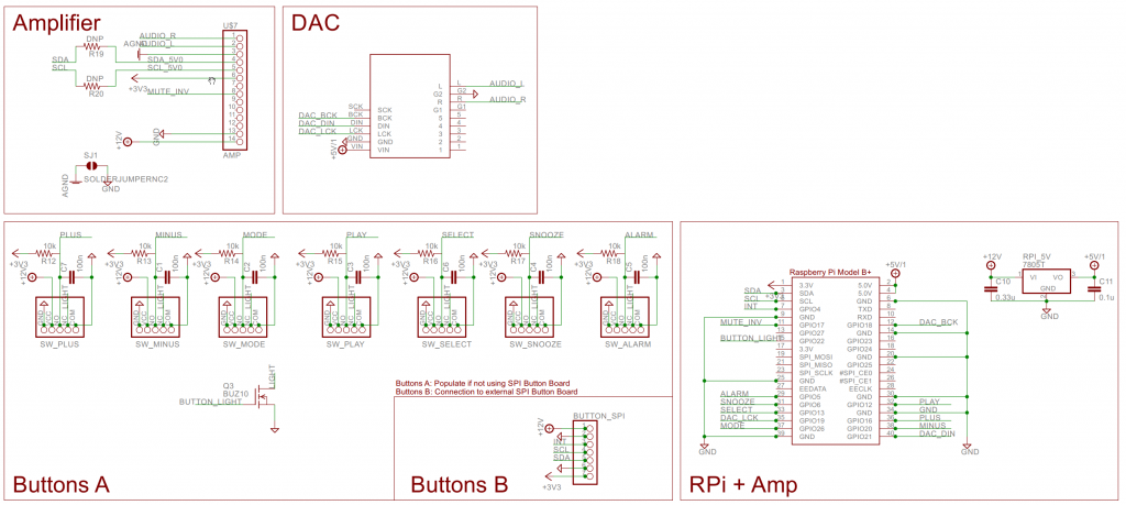
This section has:
The Raspberry Pi itself — note that the footprint says “Raspberry Pi Model B+”, but is actually sized for the Pi Zero W. I recycled an existing symbol because the header pinout is the same across both versions of the Pi, and simply forgot to rename it in Eagle. It also specifies a 7805 5V regulator to power the Pi off the input 12V bus. In practice I used a drop in switch mode replacement for the 7805 from Murata.
The button interfaces — supports two options to connect buttons. The first one, Buttons A, is for directly connecting to the motherboard. I used this option in the first two prototypes and decided to keep the option open here in case the button breakout board had problems, since I had the board space. The button connections here include a provision for +12V to illuminate the buttons, a shared switched ground line to control button illumination, resistors to pull up the buttons and caps for debounce.
Buttons B is a header for the button board, shown later. It breaks out the I2C bus connected to the RPI as well as a 3.3V rail for powering an offboard IC and a 12V rail for powering button illumination. Finally it has an interrupt pin so that the Pi can detect when the button board needs to be polled.
Finally it has footprints for I2S DAC (sound card) and Adafruit class-D amplifier. Not too much to see there.
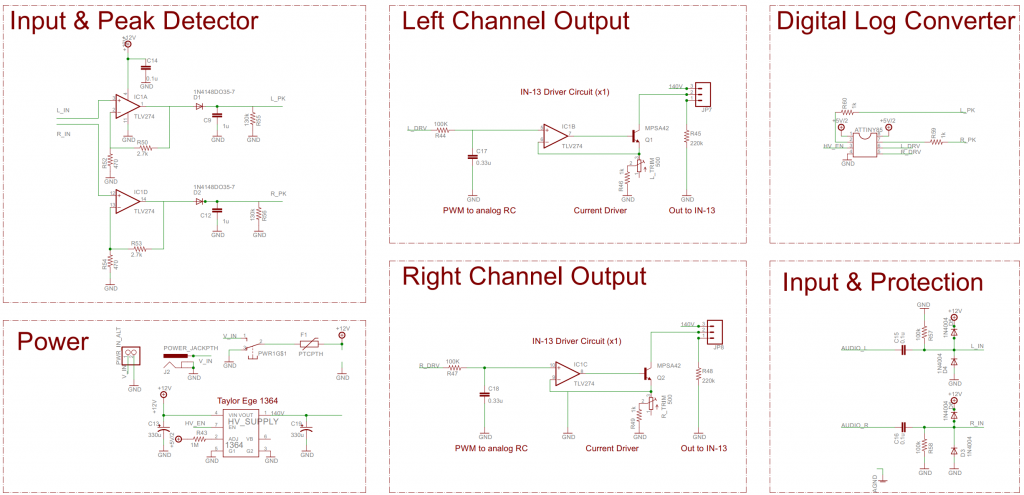
The next page of the schematic is a direct copy of my IN-13 VU Meter circuit. I won’t go into a full description of the theory, but it uses a quad rail to rail op-amp to save parts (I usually populate with an LMC660), and MPSA42 high voltage small signal transistors to drive the IN-13s. There is also an ATTINY85 micro running this code to make it act as a log converter. This saves parts and board area vs an analog implementation as well as allowing the VU meter to go to sleep if there’s been no audio for a couple of minutes.
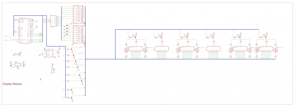
The third page of the schematic covers the Nixie display. This design was inspired by Dave Jones’ (of EEVBlog) Nixie tube driver design, which attempts to save transistors by using multi transistor ICs. Ultimately, I’m not very happy with that part of the design as there seems to be enough leakage that minor ghosting is visible on the tubes. I’ll definitely revisit it for my next Nixie project.
The controller for the display is a Teensy 3.2 which accepts commands to display values on the Nixies and INS-1 neon lamps via I2C and supports crossfading between digits.
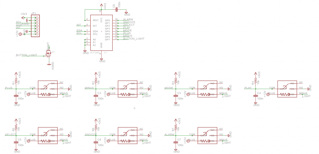
Finally, The button board uses an I2C GPIO expander IC to provide the same functionality as the individual button headers shown earlier, but without having nearly as many wires. The downside is that it requires an extra IC to do the job, and once the buttons are in the case, they’re soldered to the PCB and are pretty much stuck for good.
Layouts
The UNIAC mainboard layout is pretty compact. There’s not too much to talk about. Most of the size was defined by the need to have the Nixies at the top, bargraph tubes in the middle, and buttons at the bottom. Except for the routing around the Nixies themselves, there were no space constrained areas. I did choose to put the Teensy and RPi near the edges, so that their USB ports were practically accessible, however.
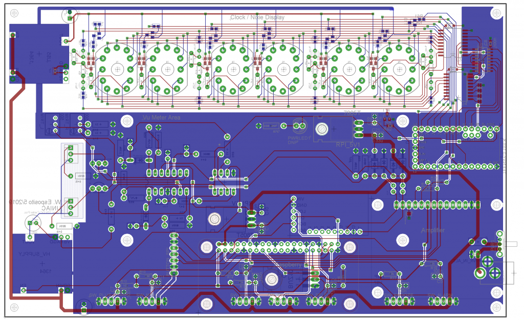
I went to great lengths to calculate minimum creepage distances and trace widths, which I used as design rules to ensure the Nixie display would be safe while being as small as I could make it. When routing my HV traces, I assumed 200 V DC and used a calculator like this one. I ended up using approximately 16mil or 0.4mm as my minimum trace clearance.
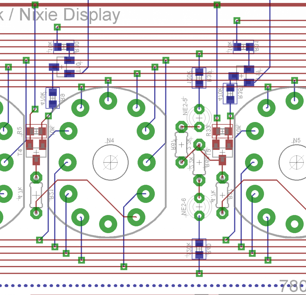
For trace width, I used 4PCB’s calculator, and found that even 600 mA would only cause a 10˚C rise for a 6 mil (0.15 mm) wide trace, way more than any of my HV traces were going to carry.vI also chose to keep the ground plane far away from the HV areas for added safety. Given that the Nixies are multiplexed and connect to ground only at a few points, it made sense and decluttered the design.
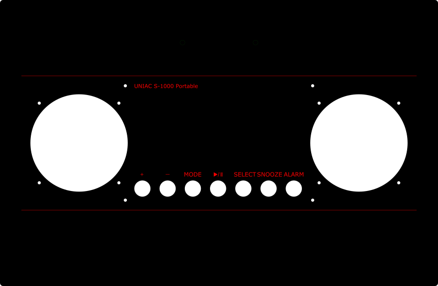
Finally, we go to the ‘Button Board’. The front panel control buttons are mounted to the front of the case and then soldered to this PCB. It’s a fairly simple design, but it has a couple of notches to clear the standoffs that mount the mainboard and speakers to the case.
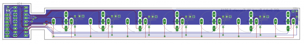
The biggest pain about this board was getting it fabricated. The buttons have wide pins that need to be fabricated as small slots. This is because the pins are so wide and closely spaced that large enough circular holes actually overlap each other.
It took three tries to get the boards fabricated. I had to make sure that the slots were on the correct layer in the footprint and had to specifically reach out to the PCB vendor in advance to ask them to send checkplots to confirm that the board would get fabbed correctly.
The first order was from AllPCB without asking in advance and they simply milled the small circular holes instead of slots. The second time, they promised that they would send me checkplots, but just fabbed the board without doing so. They also ignored my customer complaint.
It was at that point that I switched to PCBWay, who provided checkplots as requested, but they actually had the slots correct on the first try, resulting in great boards. My only regret is that their matte black soldermask is slightly shinier than AllPCB’s so the boards don’t quite match the mainboard.
The Eagle files for the switch board and main board can be found here.
BOM
The bill of materials, that is, the list of all the components used, is fairly long. It lists all the components that go on the main board, as well as the button board, and all of the off board components that I could think of. Since it’s a big, ugly table, I’m just going to attach it as a csv. The major parts themselves are detailed in the first UNIAC post.
Anyway, the full BOM can be found here.
Enclosure
Making the enclosure was a blast. My workflow is terrible and costs me several pieces of plastic on each new design I come up with, to be honest. I design the acrylic pieces as 2D Inkscape images and handle the ‘3D Modeling’ in my head. It’s even lower rent than DaveCAD!
A raw, laser-cut friendly Inkscape SVG file can be found here, with the front and back on various layers.
Conclusion
Well folks, that’s the hardware in a nutshell. The software will be another post.
It uses robotic voice announcements but they didn’t call it the Ultimate Nixie Internet Voice Alarm Clock?
I actually specifically avoided the “UNIVAC” acronym because I wanted to give it a unique name, but still have the general feel of an old-timey computer name.